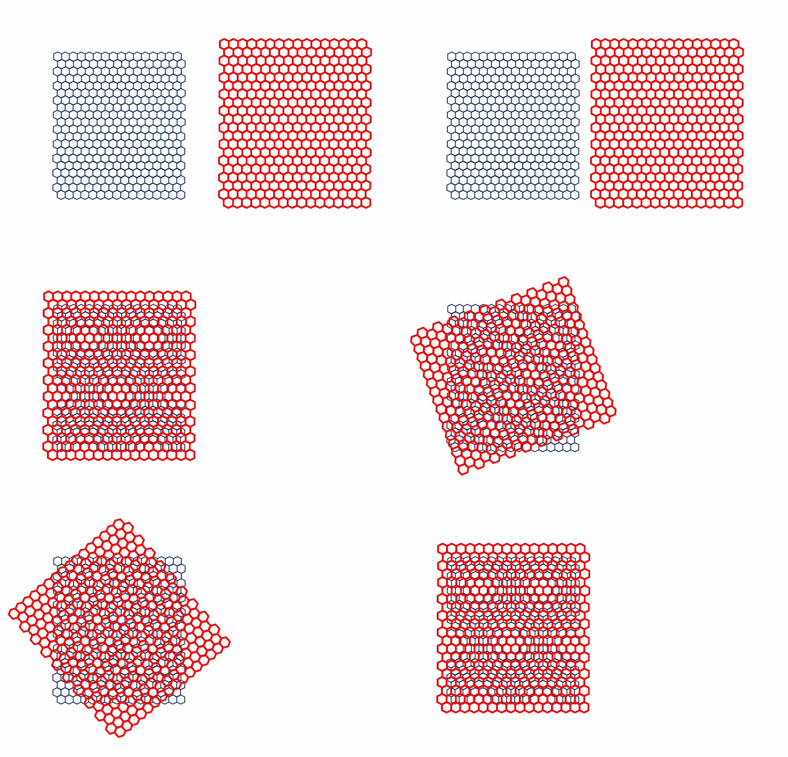
Materials that have excess electrons are typically conductors. However, moiré patterns — interference patterns that typically arise when one object with a repetitive pattern is placed over another with a similar pattern — can suppress electrical conductivity, a study led by physicists at the University of California, Riverside, has found.
In the lab, the researchers overlaid a single monolayer of tungsten disulfide (WS2) on a single monolayer of tungsten diselenide (WSe2) and aligned the two layers against each other to generate large-scale moiré patterns. The atoms in both the WS2 and WSe2 layers are arranged in a two-dimensional honeycomb lattice with a periodicity, or recurring intervals, of much less than 1 nanometer. But when the two lattices are aligned at 0 or 60 degrees, the composite material generates a moiré pattern with a much larger periodicity of about 8 nanometers. The conductivity of this 2D system depends on how many electrons are placed in the moiré pattern.
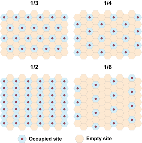
“We found that when the moiré pattern is partially filled with electrons, the system exhibits several insulating states as opposed to conductive states expected from conventional understanding,” said Yongtao Cui, an assistant professor of physics and astronomy at UC Riverside, who led the research team. “The filling percentages were found to be simple fractions like 1/2, 1/3, 1/4, 1/6, and so on. The mechanism for such insulating states is the strong interaction among electrons that restricts the mobile electrons into local moiré cells. This understanding may help to develop new ways to control conductivity and to discovery new superconductor materials.”
Study results appear today in Nature Physics.
The moiré patterns generated on the composite material of WS2 and WSe2 can be imagined to be with wells and ridges arranged similarly in a honeycomb pattern.
“WS2 and WSe2 have a slight mismatch where lattice size is concerned, making them ideal for producing moiré patterns,” Cui said. “Further, coupling between electrons becomes strong, meaning the electrons ‘talk to each other’ while moving around across the ridges and the wells.”
Typically, when a small number of electrons are placed in a 2D layer such as WS2 or WSe2, they have enough energy to travel freely and randomly, making the system a conductor. Cui’s lab found that when moiré lattices are formed using both WS2 and WSe2, resulting in a periodic pattern, the electrons begin to slow down and repel from each other.
“The electrons do not want to stay close to each other,” said Xiong Huang, the first author of the paper and a doctoral graduate student in Cui’s Microwave Nano-Electronics Lab. “When the number of electrons is such that one electron occupies every moiré hexagon, the electrons stay locked in place and cannot move freely anymore. The system then behaves like an insulator.”
Cui likened the behavior of such electrons to social distancing during a pandemic.
“If the hexagons can be imagined to be homes, all the electrons are indoors, one per home, and not moving about in the neighborhood,” he said. “If we don’t have one electron per hexagon, but instead have 95% occupancy of hexagons, meaning some nearby hexagons are empty, then the electrons can still move around a little through the empty cells. That’s when the material is not an insulator. It behaves like a poor conductor.”
His lab was able to fine-tune the number of electrons in the WS2- WSe2 lattice composite in order to change the average occupancy of the hexagons. His team found insulating states occurred when average occupancy was less than one. For example, for an occupancy of one-third, the electrons occupied every other hexagon.
“Using the social distancing analogy, instead of a separation of 6 feet, you now have a separation of, say, 10 feet,” Cui said. “Thus, when one electron occupies a hexagon, it forces all neighboring hexagons to be empty in order to comply with the stricter social distancing rule. When all electrons follow this rule, they form a new pattern and occupy one third of the total hexagons in which they again lose the freedom to move about, leading to an insulating state.”
The study shows similar behaviors can also occur for other occupancy fractions such as 1/4, 1/2, and 1/6, with each corresponding to a different occupation pattern.
Cui explained that these insulating states are caused by strong interactions between the electrons. This, he added, is the Coulomb repulsion, the repulsive force between two positive or two negative charges, as described by the Coulomb's law.
He added that in 3D materials, strong electron interactions are known to give rise to various exotic electronic phases. For example, they likely contribute to the formation of unconventional high temperature superconductivity.
“The question we still have no answer for is whether 2D structures, the kind we used in our experiments, can produce high temperature superconductivity,” Cui said.
Next, his group will work on characterizing the strength of the electron interactions.
“The interaction strength of the electrons largely determines the insulation state of the system,” Cui said. “We are also interested in being able to manipulate the strength of the electron interaction.”
Cui and Huang were funded by grants from the National Science Foundation, a Hellman Fellowship, and a seed grant from SHINES.
They were joined in the research by Tianmeng Wang, Shengnan Miao, Zhipeng Li, Zhen Lian and Su-Fei Shi at Rensselaer Polytechnic Institute in New York; Chong Wang and Di Xiao at Carnegie Mellon University in Pennsylvania; Takashi Taniguchi and Kenji Watanabe at the National Institute for Materials Science in Japan; and Satoshi Okamoto at Oak Ridge National Laboratory in Tennessee. Huang, T. Wang, Miao, and C. Wang contribute equally to the study.
The research paper is titled “Correlated Insulating States at Fractional Fillings of the WS2/ WSe2 Moiré Lattice.”
(Header image: Xiong Huang (left) and Yongtao Cui. Credit: Microwave Nano-Electronics Lab, UC Riverside.)


